Band structure engineering in 3D topological insulators
Topological p-n junction
Three-dimensional strong topological insulators (TIs) of the family Bi2Se3, Bi2Te3, Sb2Te3, and their alloys, have been widely studied over the past decade. In order to enable their future applications for spintronics, it is mandatory to obtain thin films of these materials with insulating volume and with the Dirac point of their topological states adjusted to the Fermi level. Our group has reported on pivotal experiments in this direction, where two different TIs were grown as a bilayer in order to create a vertical topological p-n junction. This way we were able to control the Fermi level position of the Dirac cone at the surface of a junction only by changing the thickness of one of the layers of the junction, which does not lead to the disorder unavoidable in the ternary compounds. Figure 1 shows atomically ordered structure of the prepared bilayers and high resolution ARPES spectra on several samples with different top layer thicknesses. Furthermore, the specific feature of the topological p-n junction, with two tunable Dirac states guaranteed on its both sides (at the surface and at the interface to the substrate), may in the future enable observation of phenomena such as topological exciton condensate, which was originally theoretically proposed in electrically gated structures.
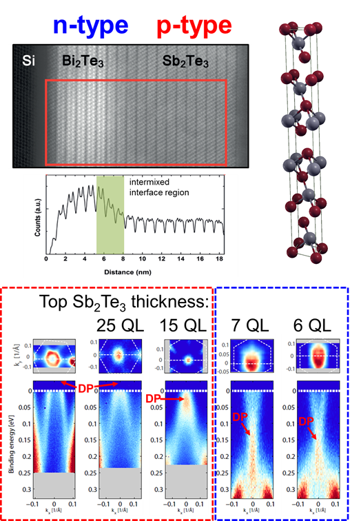
Figure 1 : Topological p-n junction. Top: STEM image of the TI bilayer grown on Si(111). Bottom: ARPES spectra showing the Dirac cone dispersion vs. the thickness of the top Sb2Te3 layer.
Publication:
M. Eschbach, E. Mlynczak, J. Kellner, J. Kampmeier, M. Lanius, E. Neumann, C. Weyrich, M. Gehlmann, P. Gospodaric, S. Döring, G. Mussler, N. Demarina, M. Luysberg, G. Bihlmayer, T. Schäpers, L. Plucinski, S. Blügel, M. Morgenstern, C. M. Schneider, and D. Grützmacher
Realization of a vertical topological p-n junction in epitaxial Sb2Te3/Bi2Te3 heterostructures
Nature Communications 6, 8816 (2015), doi: 10.1038/ncomms9816
Bi1Te1: a dual topological insulator
Realization of the topological p-n junction presented in Fig. 1 was possible due to the van-der-Waals epitaxy of one pure binary TI compound (Sb2Te3) on top of the other (Bi2Te3). New fascinating properties emerge when the regular quintuple layer stacking of 3D TIs is interrupted in binary compounds of other stoichiometeries while, ideally, retaining bulk band insulator properties. We have identified such scenario in the Bi1Te1 phase, where two quintuple layers of Bi2Te3 are combined with a single Bi-bilayer to form a natural superlattice phase. Bi1Te1 is not a strong topological insulator, but it is simultaneously a weak topological insulator (WTI) and a topological crystalline insulator (TCI). Topologically non-trivial crossing protected by the crystal symmetry away from the time-reversal invariant momentum (TRIM) point for Bi1Te1 is presented in Fig. 2 indicating its TCI character.
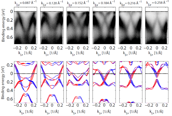
Figure 2: ARPES off-normal emission spectra and theoretical calculations for the surface of the Bi1Te1 natural superlattice.
Publication (under review):
M. Eschbach, M. Lanius, C. Niu, E. Mlynczak, P. Gospodaric, J. Kellner, P. Schüffelgen, M. Gehlmann, S. Döring, E. Neumann, M. Luysberg, G. Mussler, L. Plucinski , M. Morgenstern, D. Grützmacher, G. Bihlmayer, S. Blügel, C. M. Schneider, Bi1Te1: a dual topological insulator, arXiv:1604.08886 (2016)
Spin textures in transition metal dichalcogenides
Transition metal dichalcogenides (TMDCs) are layered quasi two-dimensional systems which exhibit number of important properties. Most widely studied and known is MoS2, a naturally occurring mineral which is sometimes termed a “semiconducting graphene” and similar compounds WSe2, MoSe2 and WSe2. With thinning down to a monolayer limit (it is a convention to call an atomic tri-layer S-Mo-S a “monolayer” of MoS2) they undergo indirect to direct band gap transition, with the valence band maximum switching from Gamma to K, and furthermore, due to the broken inversion symmetry in the monolayer, spin-momentum locking with opposite spin textures at the inversion asymmetric K and K’ points is exhibited. In the bulk of the material, in the case of the most common 2H polytype (A-B-A stacking), the inversion symmetry is retrieved, however, locally within each separate monolayer it is still broken. This leads to the spin layer locking, and the so-called “hidden spin polarization” in the inversion-symmetric crystals (when averaging the entire primitive cell, the combination of time-reversal symmetry and inversion symmetry prohibits spin polarization). Therefore, due to the surface sensitivity of photoemission, it is possible to observe high spin polarization at the K-bar point, and it reversal at the K’-bar point for 2H MoS2 single crystal, assuming that the terrace width is larger compared to the diameter of the photon beamspot. The results of our group are presented in Fig. 3, where the quasi two-dimensional character of the states at K-bar is observed in high-resolution ARPES spectra with high spin-polarization, reversed between K-bar and K’-bar points in spin-polarized ARPES. Such results could have been observed in the 3R polytype of MoS2 (the A-B-C stacking), however, this is not the case, since the size of the spin-splitting at K-bar is in perfect agreement with previously measured values for the 2H polytype, which is in agreement with further characterizations we have performed using AFM (macroscopically large terraces) and with reflectivity measurements. The property of spin-polarized valleys (for holes) at K and K’ led to the term “valleytronics”, a field where these properties are utilized e.g. in optical effects (e.g. circular polarization detection).
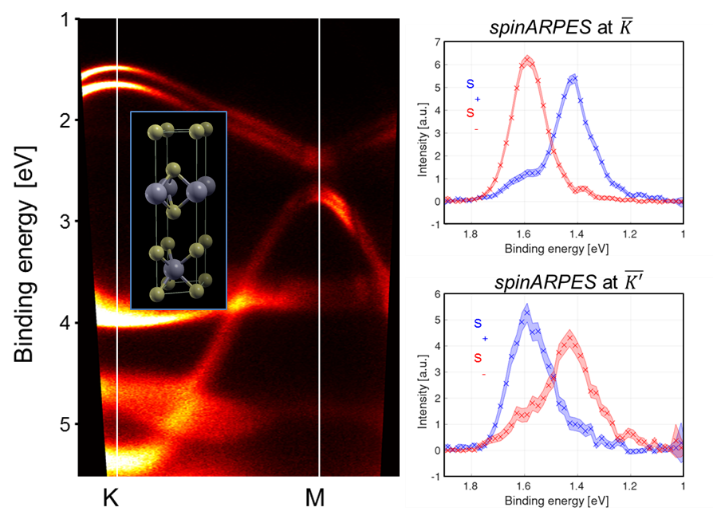
Figure 3: Spin-polarized ARPES from MoS2 single crystal. Left panel shows E(k) map along the bar-KM direction of the Brillouin zone, right panel shows the reversal of the spin polarization between K-bar and K’-bar points. Inset in the left panel shows the unit cell of 2H MoS2.
Publication:
M. Gehlmann, G. Bihlmayer, I. Aguilera, E. Mlynczak, M. Eschbach, S. Döring, P. Gospodaric, S. Cramm, B. Kardynal, L. Plucinski, S. Blügel, and C. M. Schneider
Quasi 2D electronic states with high spin-polarization in centrosymmetric MoS2 bulk crystals
Scientific Reports 6, 26197 (2016), doi:10.1038/srep26197
Fermi surface manipulation in a prototypical ferromagnet
Spin-orbit coupling (SOC) is often considered “small” and is routinely neglected when considering the electronic band structure of Fe, Co, and Ni transition metals. Instead, ab-initio calculations of Fe predict opening and closing of SOC-related gaps of 100 meV or more, for the otherwise equivalent directions along the magnetization and orthogonal to the magnetization. These effects can be studied in high quality of Fe(001) thin films grown on Au(001). In order to achieve high crystalline quality, these films are grown at cryogenic temperature to suppress Au segregation to the surface during growth, and then only mildly annealed. ARPES spectra in Fig. 4 show how SOC breaks the symmetry in the band structure of Fe. These are essential electronic fingerprints of the fundamental magnetic phenomena such as magnetocrystalline anisotropy and x-ray magnetic linear dichroism. Moreover, the detected electronic band gaps might play a substantial role in the spin transport effects, such as tunneling anisotropic magnetoresistance (TAMR). More detailed analysis of these results with the aid of one-step modeling of photoemission signal reveals additional influences due to magnetic dichroism effects in photoemission, and due the localization of the wave functions in the surface region, in agreement with the Rashba-type effect.
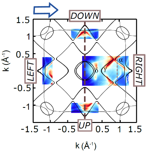
Figure 4: Spin-orbit coupling effects in the electronic structure of Fe thin film. Experimental Fermi surface cuts (measured at 16.7 eV photon energy) for the four in-plane magnetization directions are shown.
Publication (under review):
E. Młyńczak, M. Eschbach, S. Borek, J. Minár, J. Braun, I. Aguilera, G. Bihlmayer, S. Döring, M. Gehlmann, P. Gospodarič, S. Suga, L. Plucinski, S. Blügel, H. Ebert, and C. M. Schneider
Fermi surface manipulation by external magnetic field demonstrated for a prototypical ferromagnet arXiv:1606.07680 (2016)